鑫景福致力于满足“高品质”江南体育网(中国)有限公司官网A订购单需求。

- 首页
- 江南体育网(中国)有限公司官网A加工
- BGA 江南体育网(中国)有限公司官网A组装
- 通孔江南体育网(中国)有限公司官网A组装
- 高频江南体育网(中国)有限公司官网A组装
- 医疗江南体育网(中国)有限公司官网A组装
- 工控江南体育网(中国)有限公司官网A组装
- 消费电子江南体育网(中国)有限公司官网A
- 储能模块江南体育网(中国)有限公司官网A
- 汽车电子江南体育网(中国)有限公司官网A
- SMT贴片加工
- DIP插件加工
- 小批量江南体育网(中国)有限公司官网A组装
- 大批量江南体育网(中国)有限公司官网A组装
- OEM代加工
- 江南体育网(中国)有限公司官网贴片加工
- 单面江南体育网(中国)有限公司官网组装
- 双面江南体育网(中国)有限公司官网组装
- LED 江南体育网(中国)有限公司官网组装
- 江南体育网(中国)有限公司官网打样组装
- 江南体育网(中国)有限公司官网制造
- DFMA服务
- 应用领域
- 生产技术
- 工厂直播
- 关于我们


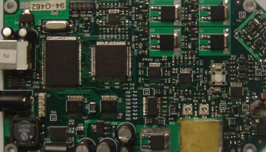
AOI inspection of DIP components before peak welding operation
Dip packaging (dual in line package), also known as two-wire online packaging technology, refers to that the manufacturer of integrated circuit chip 江南体育网(中国)有限公司官网A packaged in the form of two-wire serial connection in DIP processing belongs to 江南体育网(中国)有限公司官网 board Now most SMAll and medium-sized integrated circuits use this packaging method, and the number of pins generally does not exceed 100; Dip packaged CPU chips have two pins, whICh need to be inserted into chip sockets with dip structure or directly inserted into 江南体育网(中国)有限公司官网 boards with the same number of welding holes and geometric layout of welding
Impregnated package chips must be inserted carefully from the chip socket to avoid SMT technicians damaging the pins during handling. DIP packaging structures include: multi-layer ceramic double line DIP, single-layer ceramic double line DIP, lead frame DIP (including microcrystalline glass seal, plastic packaging structure, ceramic low melting glass packaging), etc.
有限公司官网A")
Automatic optical inspection
Post processing welding of DIP chip is a process after SMT chip processing (except for special cases: 江南体育网(中国)有限公司官网 boards with only DIP chip). The processing flow is as follows:
1. Component pretreatment
The workers in the pre processing workshop will pick out the materials in the BOM according to the BOM bill of materials, carefully check the type and specification of the materials, sign, pre process according to the model before production, and use the automatic bulk capacitor foot shearing machine and other molding equipment for processing, transistor automatic molding machine and automatic belt molding machine.
requirement:
(1) The pin leveling width of the adjusting part must be the same as that of the locating hole, with a tolerance less than 5%;
(2) The distance between component pin and 江南体育网(中国)有限公司官网 pad should not be too large;
(3) If required by the customer, molded parts are required to provide mechanical support to prevent 江南体育网(中国)有限公司官网 pad warping.
2. Paste high temperature adhesive tape, enter the 江南体育网(中国)有限公司官网 board to paste high temperature adhesive tape, block the tin plated through-hole and the components that must be welded on the back;
3. The DIP parts processing workers must wear electrostatic bracelets to prevent static electricity. Parts shall be processed according to the BOM of parts and components and the dot matrix diagram of parts and components. Smt tip handling operators must be careful not to make mistakes or leaks when inserting.
4. The operator must check the inserted parts, mainly to check whether they are inserted incorrectly.
5. For 江南体育网(中国)有限公司官网 boards with no problems, the next step is wave soldering. Wave soldering can be used to weld omnidirectional automatic 江南体育网(中国)有限公司官网 boards and curing components.
6. Remove the high-temperature adhesive tape and check it. In this link, the main step is to visually check whether the welded 江南体育网(中国)有限公司官网 is well welded.
7. For 江南体育网(中国)有限公司官网 boards that are not completely welded after inspection, repair them to prevent problems.
8. Post welding is a set of procedures for parts with special requirements, because according to its own process and data limitations, some parts cannot be directly welded by the peak welder, which needs to be manually completed by the operator.
9. For all component 江南体育网(中国)有限公司官网 circuit board pads on the, this 江南体育网(中国)有限公司官网 needs to perform a function test after the test. 江南体育网(中国)有限公司官网 bonding is completed to test whether each function is in a normal state. If a defective function is detected Workers need to identify pending process 江南体育网(中国)有限公司官网 boards immediately before repair and retest


抖音二维码

Q Q二维码

微信二维码
点击
然后
联系
然后
联系
电话热线
13410863085Q Q

微信

- 邮箱